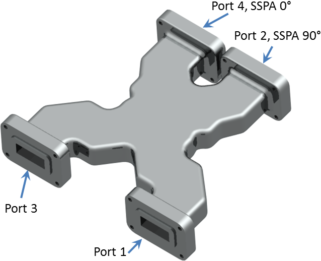
This waveguide is used to combine the output of two SSPA amplifiers. The interaction between electromagnetic waves with the geometry is studied. An optimal design can be found.
Initial Situation
Study Impact of Wave Interactions
The waveguide to be analyzed in this example is a WR42 standard model with a four port combining junction. It is used to combine the output power of two 20 GHz solid state power amplifiers (SSPA). The outputs of the two amplifiers are fed into ports 2 and 4 with a 90° out of phase separation to steer the output power of the SSPAs to port 1. Port 3 of the waveguide is the isolated port where the impedance mismatch at the output port 1 is absorbed. The waveguide is of aluminum boundary.
Goal is to find the electromagnetic wave pattern under the given conditions and to investigate the effect of wave absorption/interaction.
 Picture: Waveguide Combiner
This problem is also described and analyzed in these two documents:
Arcioni, Paolo, Perregrini, Luca, Bonecchi, Fulvio, “Low-Loss Waveguide Combiners for Multidevice Power Amplifiers,” The Second International Conference on Electromagnetics in Aerospace Applications, September 1991.
Getting Started with HFSS: A 20 GHz Waveguide Combiner
Appropriate Method
3D Full Wave Frequency Solution
Because the wavelength at 20 GHz is about the size of the geometry it is necessary to solve the full set of Maxwell equations without simplifications as it is performed by the NX Magnetics solution-type Full Wave. The solution can be solved in the time- or frequency domain. While solving in frequency domain will result in the pattern of the fully established waves the time domain solution would allow investigating the starting conditions and the detailed behavior of the oscillating field. The solver can do both and it is a good idea to compare the results of them. Following we use the frequency domain solution.
Creation of the FEM model in NX is quite simple: The inside geometry is hex-meshed and the material Air is assigned to it.
 Picture: Mesh for the Waveguide Combiner
Next step is the definition of the two incoming wave ports in the NX simulation file. For this some parameters have to be defined to describe the wave patterns on the faces. Next picture shows the resulting electric fields on the two incoming ports and the phase shift.
 Picture: Incoming Port Definition. The right Port is 90° shifted
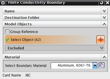
At the boundary faces of the waveguide we apply an impedance-condition Finite-Conductivity-Boundary that allows modeling the outside walls having properties of aluminum.
 Picture: Dialog for the Definition of the Boundary Material
Result
Wave Field Pattern, Absorbtion
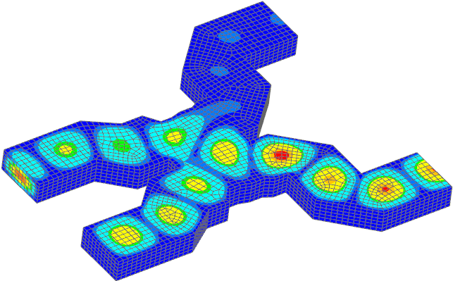
Some of the results are the real and imaginary part of electric and magnetic field patterns. These fields allow detailed investigation and understanding of the wave interaction in the given geometry. Of course the parametric NX model allows fast and easy design changes and simulation updates.
 Picture: Real Part of the Electric Field in the Waveguide


